
Wafer-level thermal integration
Diamond cooling for the age of AI.
Where semiconductor performance meets thermal freedom.
Diamontronics develops GaN-on-Diamond bonding and wafer-level thermal solutions for high-power semiconductors.
Thermal freedom
Heat should not decide how fast the future can compute.
We move the thermal bottleneck from the system level to the material interface.
See the architecture ↘Material evidence · ~300 K
Diamond changes the thermal ceiling.
Its conductivity can exceed copper by roughly five times—but only if the bond lets heat cross the interface.

Heat path
From GaN hotspot into diamond.
The active region generates heat; a thin, uniform bond transfers it into the diamond heat spreader.
Diamond
1000–2200
3C-SiC
>500
Copper
≈400
AlN
≈237
GaN
≈200
Representative bulk values near room temperature. Films, crystal quality and interfaces vary by process.
High-k material is only half the solution.
Interface resistance can dominate the total thermal path. Bonding quality determines how much of diamond's material advantage reaches the device.
See how we engineer the interface ↘Technology
Heat limits GaN. Diamond changes the path.
A wafer-level process platform designed to move heat away from the active device faster.


Wafer-level architecture
GaN + Diamond
RTH
10 K·mm/W
Damage-free room-temperature bonding
Atomic-level interfacial contact without a conventional thick intermediate layer.
Plasma-assisted diamond polishing
Surface roughness reduced to 0.3 nm for high-quality wafer integration.
Fs-laser thermal post-processing
A process route designed to enhance heat dissipation efficiency by 25%.
Offerings
From materials to integrated devices.
Products
GaN-on-Diamond wafers, substrates and future packaged products.
↗Technical services
Bonding, polishing, process verification and engineering development.
↗Chips
Reference devices and future chip-level customer programs.
↗Applications
Built for the highest-value GaN markets.
Aerospace & defense
Strategic systems where thermal performance defines capability.
5G-A / 6G & satellite
Base stations, RF infrastructure and satellite payloads.
AI server & data center
High-power computing with rapidly growing cooling demand.
Power electronics
eVTOL, robotics and next-generation electric mobility.
About
From diamond science to wafer-scale impact.
Diamontronics was founded to commercialize diamond thermal dissipation for next-generation wide-bandgap semiconductors.

Founder
Prof. Yang Lu
Chair Professor and Associate Dean at HKU, with 20 years of experience in micro-nanomechanics and diamond/semiconductor advanced manufacturing.
News & milestones
Proof of concept. Built for scale.
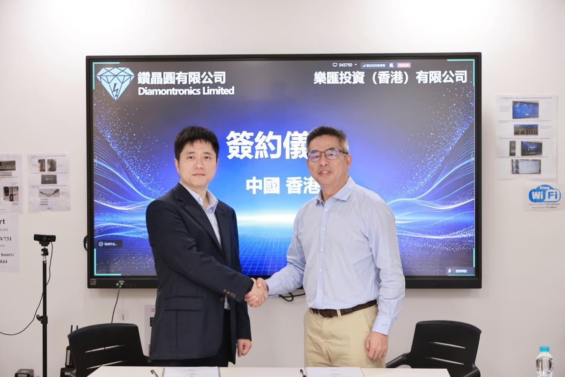
2026 · Financing milestone
Diamontronics completes proof-of-concept financing round.
The financing will accelerate process validation for chip-level diamond thermal solutions and the development of atomic-scale ultra-precision polishing equipment.
Registered in 2023
Hong Kong Science Park since 2025
Chip-level diamond thermal management
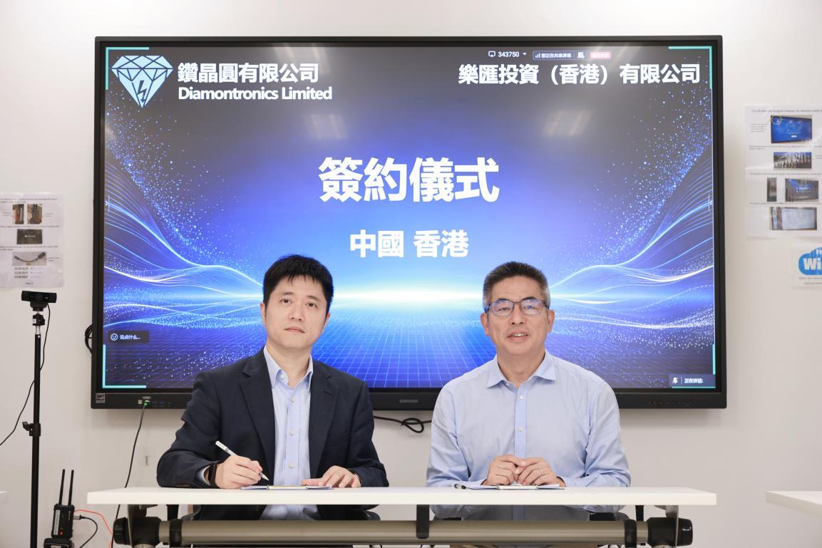
Signing ceremony · Hong Kong
From proof of concept to wafer-level process validation.
The agreement marks the next stage of Diamontronics' chip-level diamond thermal management program.
Ideas
Have an idea for how GaN-on-Diamond can change the world?
Share a breakthrough application with us. Together, we can push high-power semiconductors into new markets.
Share your ideaContact
Let’s build the next thermal platform.
Room 1035, 10/F, 19W Building, Hong Kong Science Park.
info@diamontronics.com